Advanced materials engineering
Technology
THE PVD TECHNOLOGY
The abbreviation PVD stands for Physical Vapor Deposition, in which the surfaces of predominantly metallic or ceramic substrates are coated with extremely thin layers in environmentally friendly vacuum processes.
This is achieved by the two different coating processes sputtering or arc evaporation, which have in common
that different materials are deposited in the gaseous state on the substrate surface.
Since the process temperatures on which these processes are based are very low and may even occur at room temperature, a structural change of steels can be ruled out.
Goals of the PVD Coating
The ultimate goal of PVD coatings, which today are among the leading technologies in terms of wear protection, friction, erosion and corrosion reduction, life extension and surface hardness improvement, is to improve the productivity, performance and quality of business production in a variety of different areas.
PVD coatings are very environmentally friendly thanks to a variety of different aspects like using only a few resources during the process and producing only small amounts of waste materials and exhaust gases. In addition, the durability and service life of the tools are significantly improved, thus protecting the environment.
Why PVD Coating Systems from KCS Europe?
Increase in productivity
Increased durability
Cost reduction
Protection of the environment

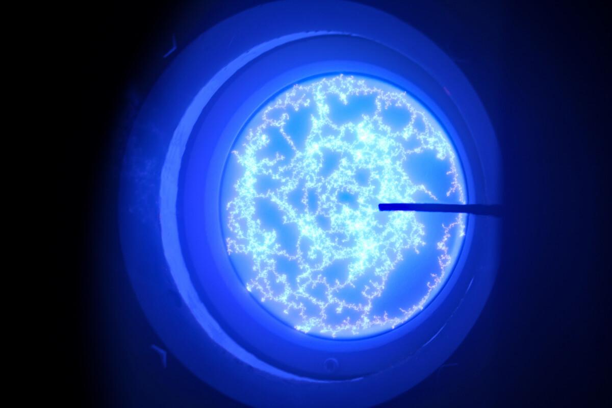
ARC
The Arc is local discharge, leading to point temperatures of about 15,000°C, evaporating the target material into the gas phase. As the gas phase exhibits neutral and ionic species it can also be considered as a plasma. Additionally, introduced reactive gas like O2 or N2allow synthesis of compound films such as typical hard coatings Al2O3 or TiN. Target species are now transported through this plasma phase and condense on a surface, typically the tool or sample, creating a thin film. While applying a potential on the sample, the so-called bias potential, ionized species in the plasma can be additionally attracted and the energetics of the incoming species can be tuned. This tuned energetics of the incoming species can be used to adjust thin film and ultimately tool/sample properties. Properties which can be adjusted in this manner are thin film structure, hardness, adhesion, stress, density, and many more.
Different power supplies enable a large variety of metallic, ceramic and compound material systems including conducting to insulating materials. The additional possibility to adjust the energetics in the process enable significantly lower process temperature compared to standard CVD (chemical vapor deposition) processes.

SPUTTERING
A gas, typically an inert gas such as Argon or Krypton, is introduced in the deposition chamber and used as sputter gas. Additionally, reactive gases such as Oxygen or Nitrogen can be introduced into the deposition chamber, allowing the synthesis of compound films such as Al2O3 or TiN. Ionized gas species are attracted by a negative potential towards the target surface, initializing the sputter process. Momentum and energy transfer while these sputter events can lead to target atom ejection. Depending on the impinging ion energy, the sputtered species can be neutral or ionized. The energetics of the neutral species can be affected by collisions during transport through the gas phase or effectively the gas pressure. Ionized species can additionally be attracted by an electric potential on the sample surface, the so-called Bias potential. Finally, controlling the energetics of the incoming species can be used to adjust thin film and ultimately tool/sample properties. Properties which can be adjusted in this manner are thin film structure, hardness, adhesion, stress, density, and many more.
Different power supplies enable a large variety of metallic, ceramic and compound material systems including conducting to insulating materials. The additional possibility to adjust the energetics in the process enable significantly lower process temperature compared to standard CVD (chemical vapor deposition) processes.